

Latest News
-

-

-

T113 External SPI NAND Storage Solution
2026-07-03 -

Ethernet Schematic Design for Allwinner T113
2026-07-03 -

Designing a High Anti-Interference Isolated RS485 Interface for Allwinner T153
1、Overview
In industrial control, smart building, power monitoring and other scenarios, the RS485 bus is widely used for its advantages of simple wiring, long transmission distance, and multi-node support. However, the electromagnetic environment on industrial sites is complex, with numerous interference sources such as motor start-stop, relay operation, and lightning surges. Ordinary non-isolated RS485 interfaces are highly prone to communication abnormalities or even chip damage caused by excessive common-mode voltage and ground potential differences. Based on the Allwinner T153 SoC, this article details how to design a highly anti-interference isolated RS485 interface across three dimensions: power isolation, signal isolation, and interface protection.
2、Power Isolation Design
2.1 Isolated Power Supply Selection
Power isolation is the energy foundation of the entire isolation system. This design uses the B0505S-1WR3 fixed-voltage input isolated power module, with 5V input, 5V output, and 1W power rating, belonging to the fixed-voltage input DC-DC isolation module category. The module features high integration and achieves 1500Vdc electrical isolation without peripheral components, providing an independent VDD_485 power supply for the RS485 side and fundamentally cutting off the DC path between the two grounds.
The selection of the 1W power level is well-considered: the typical operating current of the SIT3088EESA transceiver is approximately 300μA, and combined with the power consumption of the digital isolator and peripheral circuits, the total power consumption is far below 1W, leaving sufficient margin. Meanwhile, a 270Ω dummy load resistor R320 is connected in parallel at the module output to ensure stable operation under light-load conditions and prevent output voltage drift.
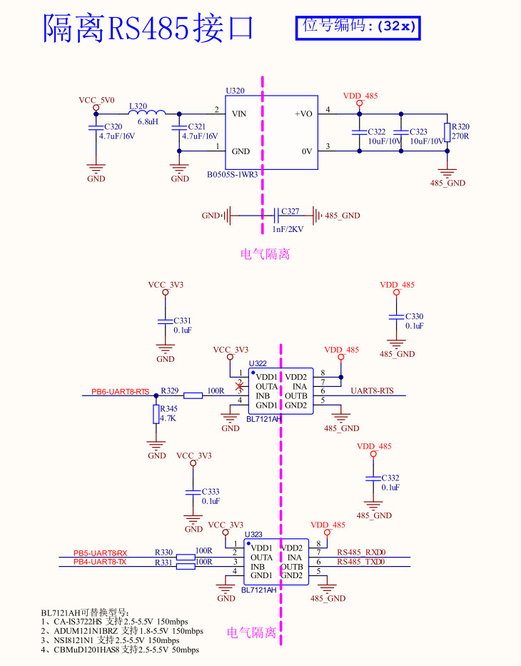
Figure 1: Power and Signal Isolation Schematic
2.2 Input and Output Filtering Design
Both the input and output terminals of the isolated power module require a complete filtering network. On the input side, VCC_5V0 first passes through an LC filter circuit composed of a 6.8μH inductor L320 and a 4.7μF capacitor C320 to suppress high-frequency noise on the power line. A 4.7μF/16V ceramic capacitor C321 is then connected in parallel near the module input pins to provide a local decoupling path.
On the output side, two 10μF capacitors C322 and C323 are connected in parallel to VDD_485, with the combination of large and small capacitance values covering ripple suppression across different frequency bands. A well-designed filter not only ensures power quality but also inhibits coupling of the module's own switching noise into the system side through the power line.
2.3 Ground-to-Ground Safety Capacitor Design
A 1nF/2KV safety capacitor C327 is connected across GND and 485_GND. The function of this capacitor is to provide a low-impedance discharge path for high-frequency common-mode interference while maintaining isolation characteristics at DC and power frequency. The 2KV voltage rating ensures the capacitor will not break down under surge impact, while the 1nF capacitance value discharges high-frequency noise without affecting isolation withstand voltage due to excessive leakage current. This capacitor is a critical component for EMC performance and must not be omitted.
3、Signal Isolation Design
3.1 Digital Isolator Selection
Signal isolation uses the BL7121AH dual-channel digital isolator to achieve electrical isolation of UART signals. The BL7121AH is a high-performance digital isolation chip supporting data rates up to 150Mbps, fully meeting the requirements of commonly used RS485 baud rates such as 115200bps and even higher.
The design also reserves multiple compatible alternative models, including CA-IS3722HS, ADUM121N1BRZ, NSi8121N1, and CBMuD1201HASS, covering different speed grades and supply chain options. Among them, ADUM121N1BRZ supports a wide voltage range of 1.8V~5.5V, NSi8121N1 supports 2.5V~5.5V, and CBMuD1201HASS is an economical choice with a 50Mbps speed grade.
3.2 Channel Configuration
The UART8 interface of the Allwinner T153 provides three signals: TX, RX, and RTS, therefore two dual-channel isolators are needed: U322 handles the RTS direction control signal, and U323 handles the TX and RX data signals. The RTS signal is used to control the transmit/receive direction of the RS485 transceiver and is key to half-duplex communication.
The VDD1 side (system side) of U322 is connected to VCC_3V3, and the VDD2 side (bus side) is connected to VDD_485, with completely independent power supplies on both sides. OUTA corresponds to the RTS output channel, bridging the system side to the bus side and controlling the enable of the RS485 transceiver. U323 is similarly configured with VDD1 connected to 3V3 and VDD2 connected to VDD_485, with OUTA for the TX direction (system to bus) and INB for the RX direction (bus to system), achieving isolated transmission of full-duplex signals.
3.3 Peripheral Circuit Design
Each isolator is equipped with 0.1μF decoupling capacitors (C331, C330, C333, C332) on both side power pins, which must be placed as close to the chip power pins as possible to provide the shortest high-frequency current path.
100Ω resistors (R329, R330, R331) are connected in series at the signal input terminals, serving current limiting and impedance matching functions while suppressing high-frequency ringing on signal lines. An additional 4.7K pull-up resistor R345 is added on the RTS signal side to ensure RTS remains high during power-up or reset, keeping the RS485 transceiver in receive mode by default and avoiding bus conflicts.
4、RS485 Interface Protection Design
4.1 Transceiver Selection and Control
The RS485 transceiver uses the SIT3088EESA, a half-duplex RS485 transceiver supporting up to 256 nodes with ±15kV ESD protection. The DE (Driver Enable) and RE (Receiver Enable) pins of the chip are shorted together and controlled uniformly by the UART8-RTS signal, achieving half-duplex direction switching.
A 10Ω resistor R324 is connected in series on the control signal path to limit drive current, slow down signal edges, and reduce EMI radiation. 10Ω resistors R325 and R323 are similarly connected in series on the A and B signal lines, providing current limiting and impedance matching.
4.2 Common-Mode Suppression and Impedance Matching
The A and B lines pass through the CUW43T-513T-AU/NC network transformer (common-mode choke) before exiting to the interface. The common-mode choke presents low impedance to differential signals (normal communication signals) and high impedance to common-mode interference, effectively suppressing common-mode noise on the bus lines and serving as a key component for improving EMC performance.
A 120Ω termination resistor R326 is connected in parallel at the bus terminal for impedance matching and signal reflection elimination. Termination matching resistors are particularly important in long-distance or high-speed communication. In this design, R326 can be optionally soldered or not depending on the actual application scenario.
4.3 Multi-Stage Surge Protection Design
The interface adopts a three-stage protection architecture, progressively discharging surge energy:
● The first stage is the gas discharge tube V320 (10G091M3SF), connected in parallel between the A/B lines and protection ground. Gas discharge tubes can withstand extremely high surge currents (kA level), serving as the first line of defense and mainly discharging high-energy surges such as lightning strikes.
● The second stage consists of TVS diode array D321 (PSM712) and SMAJ6.5CA, which clamp the residual surge voltage after the first stage, limiting the voltage to a range the chip can withstand. PSM712 integrates two TVS diodes specifically designed for RS485 A/B line protection.
● The third stage is the self-recovering fuses F320 and F321 (JK-NSMD020-30V) at the interface, with a rated current of 200mA. When an overcurrent fault occurs, the fuses enter a high-resistance state to limit current, and automatically recover after the fault is cleared, protecting downstream circuits against overcurrent damage.
Additionally, 100pF capacitors C328 and C329 (marked as NC in the design, optionally soldered based on EMC test results) are connected in parallel between the A/B lines and 485_GND for filtering high-frequency common-mode noise. This multi-stage combined protection of "gas discharge tube + TVS + fuse + common-mode choke" enables the interface to withstand stringent surge and EFT tests.
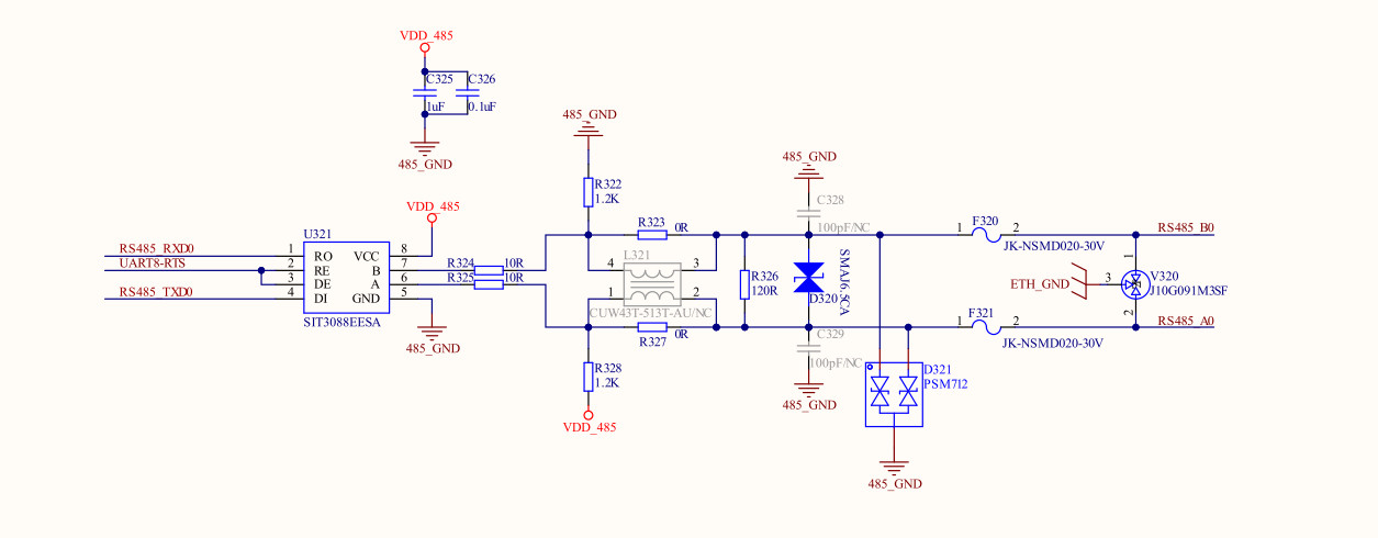
Figure 2: RS485 Transceiver Circuit
5、Summary
A highly anti-interference isolated RS485 interface requires the coordinated design of power isolation, signal isolation, and interface protection. Power isolation provides electrical isolation at the energy level, signal isolation ensures safe transmission of control and data signals, and multi-stage protection circuits directly face various interference impacts on the bus side. This design solution based on the Allwinner T153 SoC, through the combination of B0505S-1WR3 isolated power supply, BL7121AH digital isolator, and SIT3088EESA transceiver, together with complete filtering and multi-stage surge protection, can operate stably and reliably in harsh industrial electromagnetic environments.
6、About Weathink
Weathink has been deeply engaged in the field of industrial communication for many years, accumulating rich practical experience in interface anti-interference design. Through power isolation, signal isolation, and multi-stage surge protection, we have in-depth understanding of every detail that affects EMC performance, and are committed to providing customers with stable and reliable industrial-grade solutions.