
Latest News


Allwinner T153 TF Card Schematic Design and Requirements
1 Introduction to Allwinner T153
Allwinner T153 is a highly cost-effective industrial-grade processor, specifically designed for fields such as general industrial interconnection, smart control, and IoT terminals. It not only possesses powerful basic computing capabilities but also stands out with its excellent environmental adaptability and 7x24-hour industrial-grade stability. In terms of interfaces, the T153 has extremely rich peripheral resources, supporting multiple mainstream communication buses, display interfaces, and storage expansions, which can easily meet the requirements for massive data interaction and multi-device connection in complex industrial scenarios. With its extremely high cost-effectiveness and high reliability, T153 provides developers with a broad design space and is the preferred platform for many industrial core boards and customized terminals.
2 Detailed Explanation of TF Card Schematic Design
Combined with actual circuit diagrams and design checklists, the schematic design for mounting a TF card (MicroSD) on the T153 needs to focus heavily on power management, signal matching, and electrostatic protection.
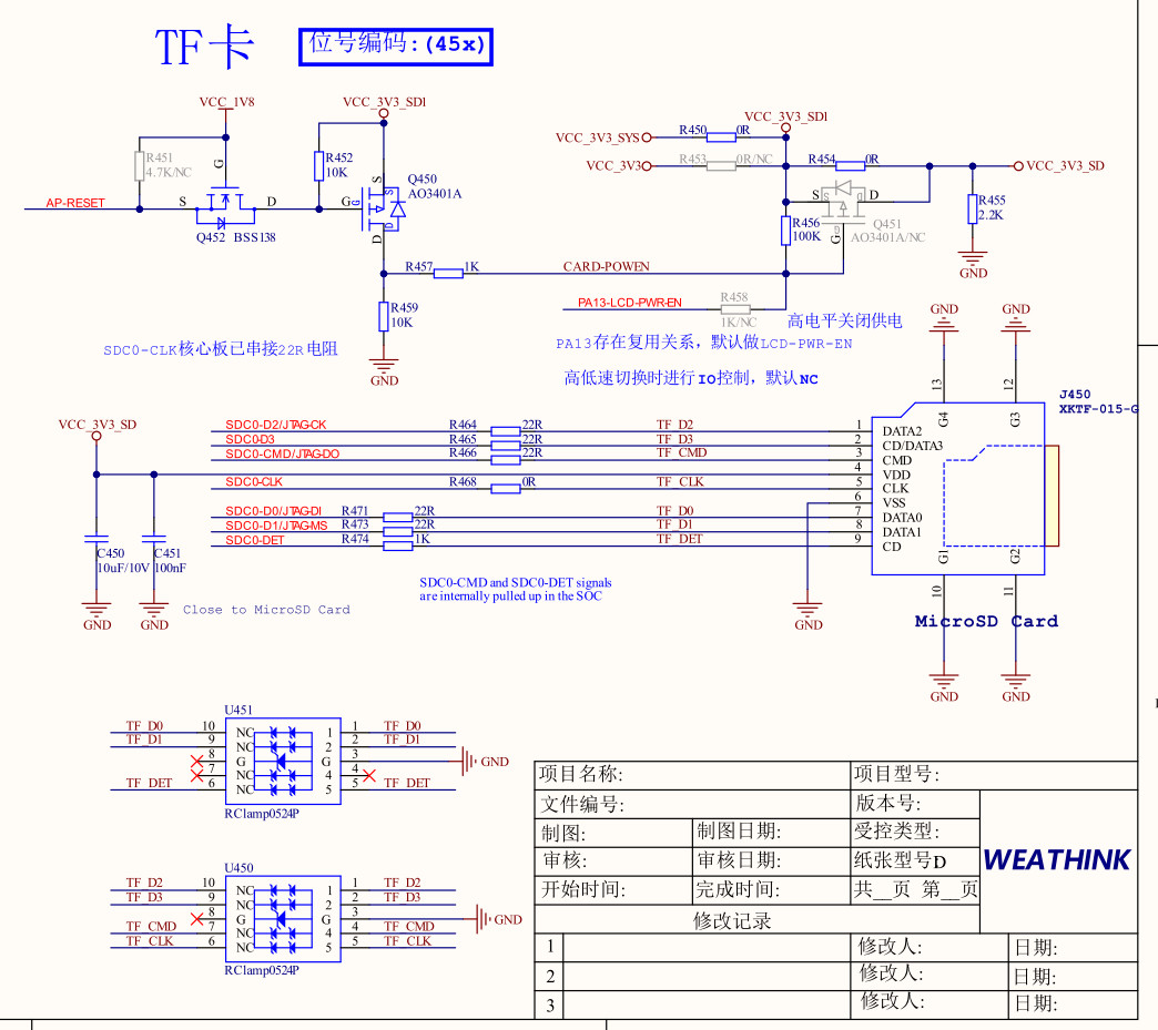
Figure 1 Schematic Diagram of T153 Connecting to TF Card
2.1 Power Control Circuit Design
To support hot-plugging and low-power management of the TF card, a MOS tube (such as Q450 AO3401A) is adopted as the power switch for the power supply section. The high and low levels are output through the main control's PA13 pin (multiplexed as LCD-PWR-EN) to control the on/off state of VCC_3V3_SD. According to design specifications, the working voltage and maximum working current of the TF card power supply must be clearly marked in the schematic, serving as a direct basis for the subsequent power trace width design in the PCB Layout.
2.2 Signal Line Configuration and Matching Resistors
The TF card interface mainly includes SDC0_CLK, CMD, D0~D3 data lines, and the DET status detection pin. The following points must be noted during design:
● Internal Pull-up: The SDC0-CMD and SDC0-DET signals have already been processed with pull-ups inside the SoC, so no redundant design is required externally.
● Clock Line Matching: Connecting pull-up resistors to the SDC0-CLK signal line is strictly prohibited. An impedance matching resistor must be connected in series (usually recommended as 33R; if a 22R resistor is already connected in series inside the core board, adjust according to the actual situation), and this resistor must be placed close to the AP (main control side).
● Data Line Matching: A 22R resistor must also be connected in series to the CMD and D0~D3 data lines to suppress signal reflection and ensure communication quality.
2.3 ESD Protection Requirements
The TF card slot is an external interface that users can directly touch, posing a high risk of electrostatic breakdown. Therefore, all signal lines of the SD interface must be equipped with ESD protection devices (such as the RClamp0524P in the diagram).
When selecting components, strict attention must be paid to the parasitic capacitance of the device: if SD 3.0 high-speed mode is supported, the ESD device capacitance of the CLK, CMD, and DATA signals must be less than 5pF; if it is only in SD 2.0 mode, it must be less than 35pF to avoid causing distortion to the high-speed signal edges.
3 PCB Layout Wiring Requirements
To ensure data integrity during high-speed reading and writing of the TF card, the Layout phase must strictly follow the rules below, and requirement annotations should be made in advance in the schematic:
3.1 Impedance and Reference Plane
The routing impedance of all TF card signal lines must be strictly controlled at 50 +/- 10% ohm. The reference plane below the routing must remain complete, and crossing split zones is strictly prohibited. Meanwhile, a spacing of 2W must be maintained between signal lines to minimize crosstalk between channels.
3.2 Equal Length Control
To ensure the accuracy of data sampling, the data lines D0~D3 and the CMD signal line require strict equal length control relative to the clock signal CLK, and the error range must be controlled within<500mil.
4 About Weathink
As a professional Allwinner solution design company, Weathink has over ten years of RD experience in high-frequency, high-speed signals and large-scale hardware. We provide highly cost-effective T153 industrial core boards and deep hardware customization services, dedicating ourselves to providing stable and reliable one-stop solutions for enterprise customers, helping industrial control and edge computing products land efficiently.