
Latest News


Schematic Design of Dual Ethernet for Allwinner T153
In industrial control, IoT gateways, and edge computing devices, dual Ethernet interface design is core to achieving internal/external network isolation, data forwarding, and redundancy backup. Based on the Allwinner T153 platform and combined with circuit design examples from Weathink, this article provides an in-depth analysis of the hardware implementation for dual Gigabit Ethernet.
1. Selection and Architecture of Ethernet Controllers
The Allwinner T153 features a built-in high-performance Ethernet MAC controller that supports the RGMII interface, allowing it to directly drive external Gigabit PHY chips.
1.1 PHY Chip Selection
In this design, two YT8531H Gigabit Ethernet transceivers (PHY) are utilized. This chip is characterized by low power consumption and high stability, fully meeting the requirements for industrial-grade applications.
1.2 Interface Bus
The MAC and PHY are connected via the RGMII (Reduced Gigabit Media Independent Interface) bus. The RGMII bus includes transmit/receive data lines, clock lines, and control signals. To ensure signal integrity, 22Ω matching resistors (such as R812-R818 in the schematic) are typically connected in series with the data lines.
2. Detailed PHY Circuit Design Analysis
The design quality of the PHY circuit directly determines the packet loss rate and stability of network communication. The following is an analysis using PHY0 and PHY1 as examples.
2.1 Power and Clock Supply
Multi-voltage Supply: The YT8531H requires multiple voltage supports. In the schematic, PHY0_AVDD33 (3.3V analog power) and PHY0_VDD10 (1.0V core power) are isolated using magnetic beads (e.g., B800/B900).
Reference Clock: Each PHY chip is connected to an external 25MHz (12pF/20PPM) passive crystal oscillator (Y800/Y900) paired with 18pF resonant capacitors to provide an accurate frequency reference for the PHY.
2.2 Hardware Configuration (Bootstrap)
The address and mode of the PHY chip are usually determined by the level status of specific pins at the moment of reset:
PHY Address Configuration: Different addresses for PHY0 and PHY1 on the MDIO bus are set via pull-up or pull-down resistors (such as R816, R819), ensuring the MAC can independently control both network ports.
Delay Configuration: By configuring the pull-up/down resistors on the RXD0/RXD1 pins (such as R801, R807), a 2ns internal delay can be enabled to compensate for timing deviations in the RGMII traces.
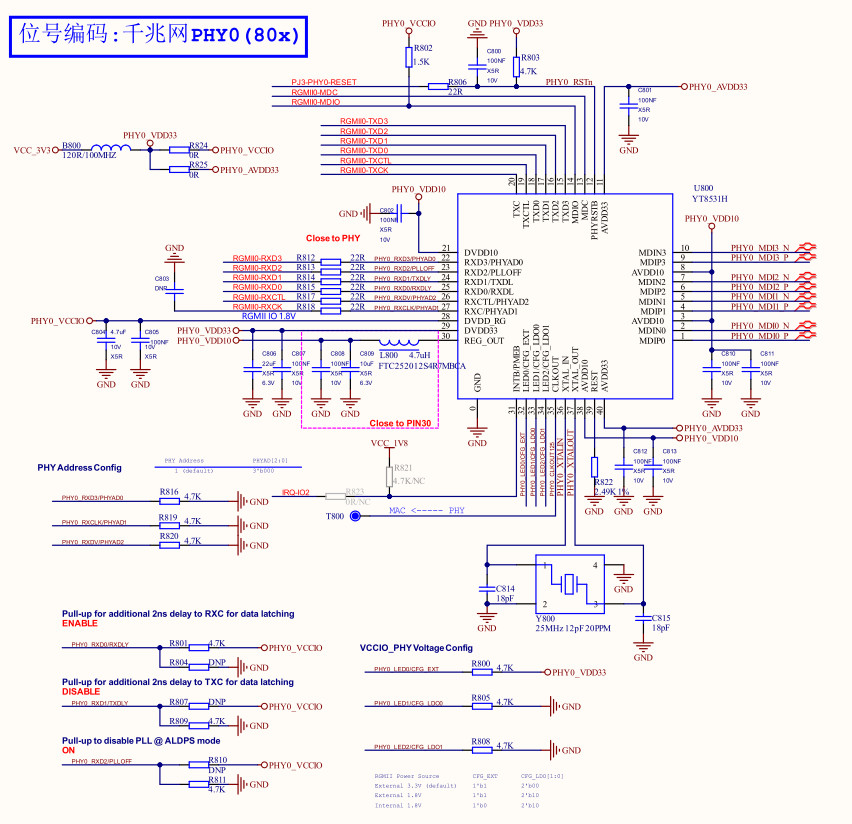
Figure 1: PHY section of the ETH0 interface
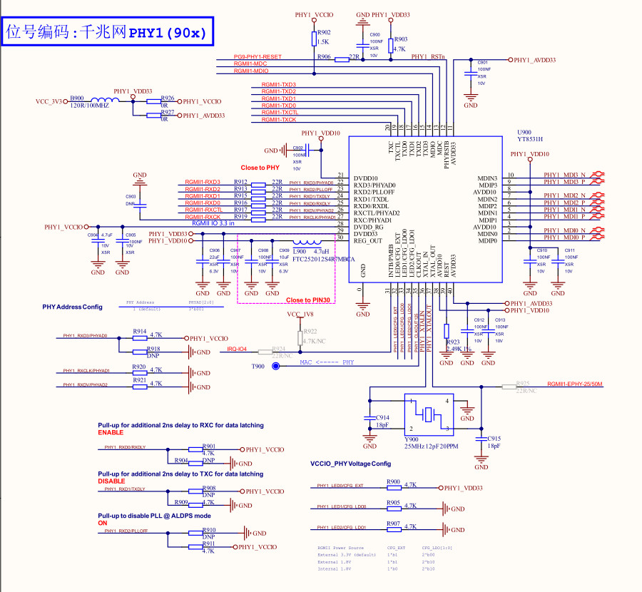
Figure 2: PHY section of the ETH1 interface
3. RJ45 Interface and Electromagnetic Compatibility (EMC) Design
Network interfaces are exposed to the exterior of the device and are highly susceptible to Electrostatic Discharge (ESD) and Surges.
3.1 Network Transformer
The design adopts a solution with integrated network transformers (such as the G2415S), whose primary functions are electrical isolation and common-mode interference suppression. The center tap of the transformer is AC-grounded through 100nF capacitors (C832-C836) to effectively filter out noise.
3.2 Interface Protection Circuit
ESD Protection: RClamp0524P TVS arrays (U831, U832) are designed on the MDI differential signal lines. This device features extremely low parasitic capacitance, providing efficient electrostatic protection without affecting Gigabit signal quality.
Chassis Ground Isolation: The RJ45 shell ground (ETH_GND) and digital ground (GND) are connected via a 1nF/2KV high-voltage capacitor (C839) and a 1MΩ resistor (R831) to discharge static electricity while maintaining electrical isolation.
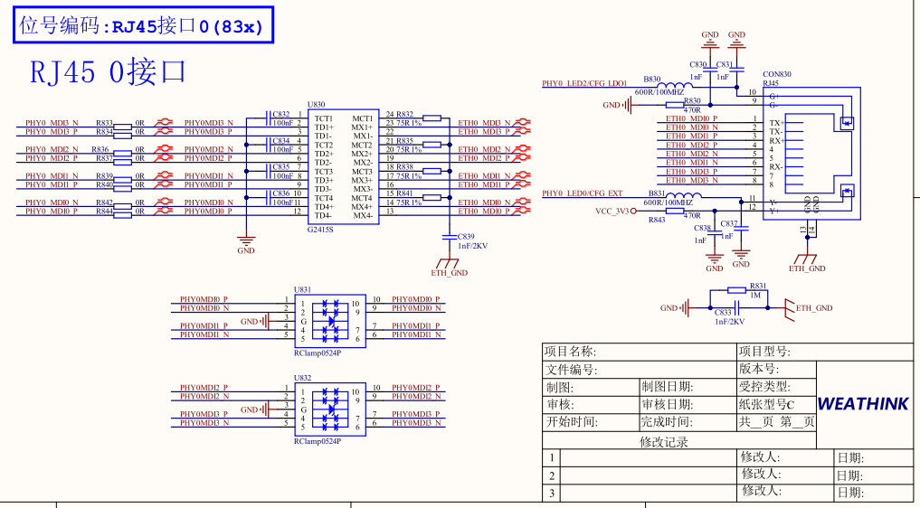
Figure 3: RJ45 section of the ETH0 interface
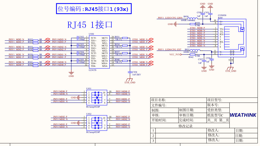
Figure 4: RJ45 section of the ETH1 interface
The above technical explanations are provided for reference; if there are any inaccuracies, feel free to contact us.
4. Weathink: Accelerating Your Product Launch
● As a veteran design house for Allwinner solutions, Weathink has been deeply involved in the field of high-performance hardware customization for many years.
● Extensive Development Experience: We possess over a decade of experience in high-speed signal routing and large-scale complex PCB design, perfectly solving timing matching and signal integrity issues for high-speed interfaces like RGMII.
● Mature Modular Design: The Allwinner T153 dual-port solution shown in this article has been validated in multiple industrial projects; the mature schematics and PCB layout solutions can be directly reused.
● One-stop Technical Support: SOM selection to customized carrier board design and driver debugging, Weathink provides technical assurance throughout the entire product lifecycle.
Choosing Weathink means choosing high cost-effectiveness and short R&D cycles, helping your products seize the initiative in a rapidly changing market