
Latest News


Hardware Design Guide for Rockchip RK3588J Implementing SATA 3.0 Connection to NGFF M.2 Hard Drives
In the fields of industrial control, edge computing, and automotive multimedia, high-speed and large-capacity storage is a core requirement. Rockchip's flagship SoC, the RK3588J, is frequently used to drive high-speed storage devices due to its powerful performance and rich interface capabilities. This article will combine actual circuit design to detail how to connect an NGFF M.2 interface hard drive via the RK3588J's PCIe 2.0/SATA 3.0 multiplexed (Mux) interface.
1. Overview of Core Protocols and Interface Standards
1.1 SATA 3.0 Protocol
● SATA 3.0 (Serial ATA Revision 3.0) is a serial interface protocol widely used for Solid State Drives (SSD) and Hard Disk Drives (HDD).
● Speed: The theoretical maximum transmission bandwidth is 6Gbps.
● Features: It features high hardware and software compatibility, supporting hot-swapping and NCQ (Native Command Queuing) technology to effectively improve random read/write performance. On the RK3588J platform, SATA 3.0 is typically multiplexed (Mux) with PCIe 2.0 signals via the Pipe PHY.
1.2 NGFF (M.2) Interface Characteristics
● NGFF (Next Generation Form Factor), now known as the M.2 interface, is a new generation interface standard specifically designed for ultra-thin devices.
● Interface Types: Common types include B Key, M Key, etc. According to the schematic (Figure 1), this design utilizes a B Key type slot.
● Transmission Capability: The M.2 interface is a physical specification that can internally carry various protocols such as SATA, PCIe, USB, HSIC, and UART.
● Speed Advantage: If using the SATA 3.0 channel, the maximum speed is 6Gbps; if using the PCIe 3.0 x4 channel (NVMe), speeds can exceed 32Gbps.
2. RK3588J Controller Side Design
In the design of the RK3588J, the PCIE20/SATA30 Mux0 module provides a flexible configuration scheme.
2.1 Signal Definition:
TX/RX Differential Pairs: SATA30_0_TXP/N and SATA30_0_RXP/N are responsible for data transmission and reception. According to the schematic, these pins are located at M34/M33 and N33/N34 of the BGA package.
2.2 Reference Clock:
Although internal clocks are typically used in SATA mode, the schematic retains the PCIE20_0_REFCLKP/N differential pair to ensure compatibility when switching to PCIe mode.
2.3 Power Supply:
The PHY circuit on the controller side requires a stable analog power supply. The diagram configures VCC_0V85_S0 (M28) and VCCA_1V8_S0 (M27), using a combination of 10uF and 1uF filtering capacitors to reduce high-speed signal interference.
2.4 Impedance Control:
For SATA 3.0 differential pairs, PCB routing must strictly control the differential impedance at 100 Ohm ±10%.
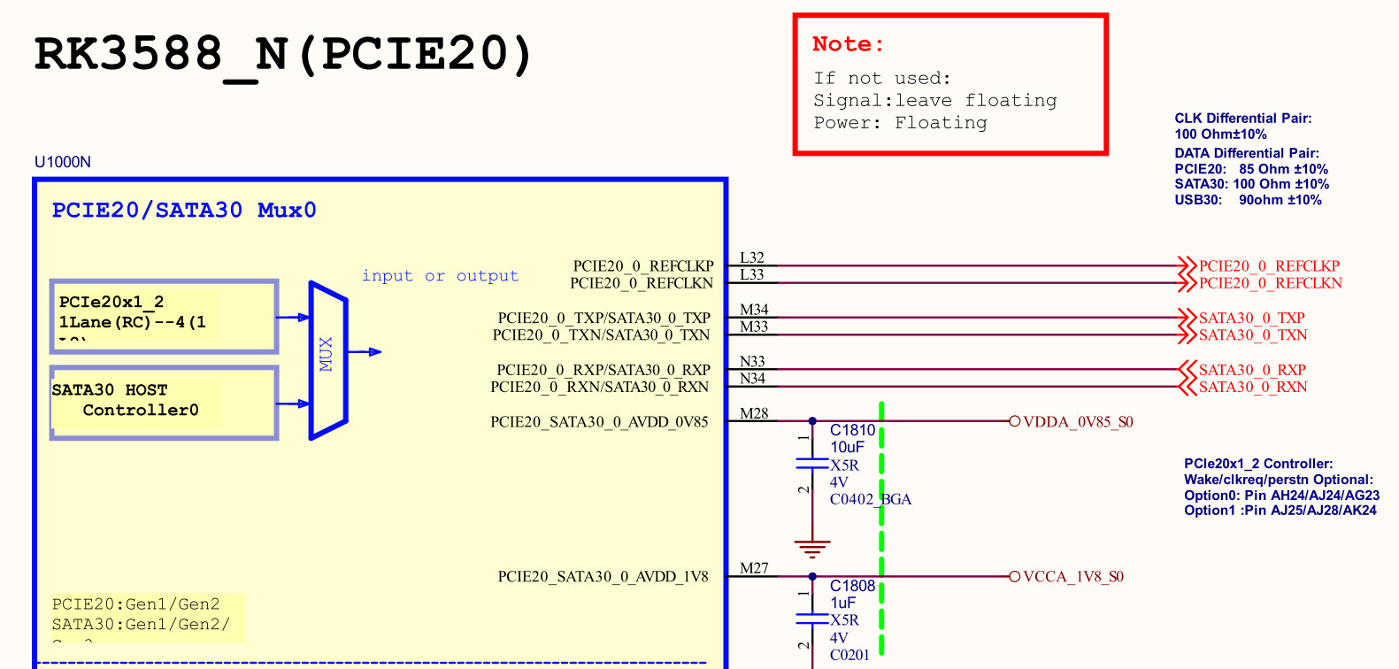
Figure 1: Controller Side Signals
3. NGFF M.2 Interface Side Design
Figure 2 shows a standard M.2 B-Key slot circuit. Its core design points are as follows:
3.1 Coupling Capacitors and Signal Connection
SATA signals must be connected in series with AC coupling capacitors before entering the M.2 connector.
Transmitter (TX): 10nF capacitors in series (C422, C423).
Receiver (RX): 10nF capacitors in series (C420, C421). The function of these capacitors is to isolate DC bias and only allow high-speed AC signals to pass, enhancing system robustness.
3.2 Power Management
M.2 hard drives have high requirements for power quality.
● 3.3V Main Power: Uses VCC_3V3_SATA for power supply. Through a filtering network (post-B420) consisting of BLM21PG600SN1D magnetic beads and multiple parallel capacitors (10pF, 33pF, 100nF, 22uF, 100uF), it ensures extremely low power ripple to meet the transient current demands of SSDs during high-speed read/write operations.
● Reset Circuit: Employs a level shifting and drive circuit composed of BSS138 MOSFETs. The RESET_L signal, after logic conversion, controls the PERSTn pin (PIN 50) of the M.2 interface, ensuring the hard drive initializes synchronously with the system.
3.3 Auxiliary Function Pins
● Config Pins: PIN 1, 21, 69, 75 are grounded through 10K resistors (R421, R423, R430, R431) for the controller to identify the type of connected device.
● Indicator Light: PIN 10 (WWAN_LED) connects to D0603_LEDG to display real-time disk read/write activity (Disk Activity).
● SMBus/I2C: Retains I2C_SCL/SDA pins for temperature monitoring or reading memory information.
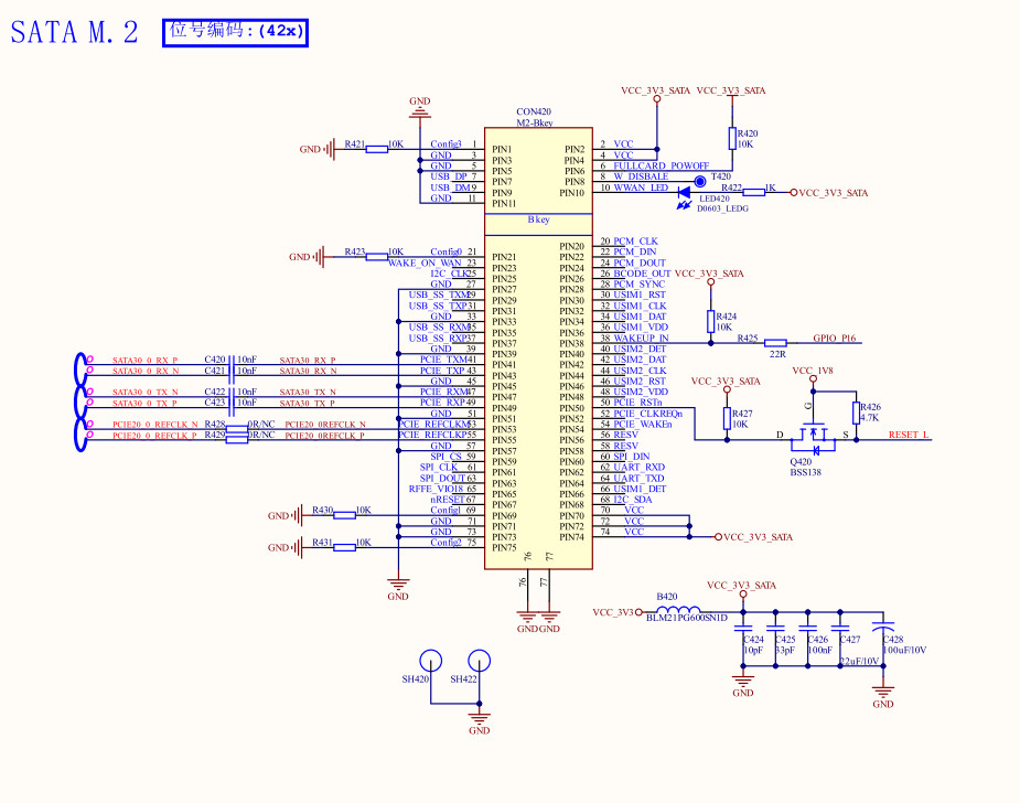
Figure 2: M.2 B-Key Interface Connection Diagram
4. Design Considerations and Summary
● Length Matching and Spacing: When routing from the RK3588J to the M.2 interface, the intra-pair length difference for TX/RX differential pairs should be controlled within 5mil, and the number of vias should be minimized.
● Power Integrity: Since the M.2 interface peak current is large, it is recommended that the power trace width be at least 40mil or handled using copper pours.
● Mode Configuration: In the software (DTS device tree), the RK3588J PHY mode must be correctly configured as PHY_TYPE_SATA to enable the SATA controller.
Through the precise design of the hardware circuits mentioned above, the RK3588J can stably drive SATA 3.0 protocol M.2 SSDs, providing a high-speed storage solution for industrial-grade applications that balances cost-effectiveness and reliability.
5. Practical Testing and Mounting
After debugging the hardware circuit, initialization and performance verification of the hard drive are required at the software level.
Formatting: Once the system identifies the device (e.g., /dev/sda), use mkfs.ext4 /dev/sda1 to format the partition into an ext4 file system.
Mounting Device: Execute the mount -t ext4 /dev/sda1 /mnt/sata_disk command to complete manual mounting.
Read/Write Verification: Test read/write speeds using the dd command or the fio tool. Due to the SATA 3.0 protocol and refined filtering design, measured sequential read/write rates should stabilize above 500MB/s, fully utilizing the 6Gbps channel performance.
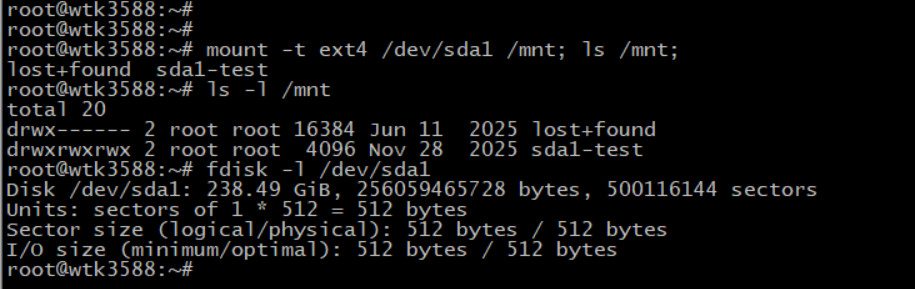
Figure 3: Actual Testing of NGFF Hard Drive
6. Solution Recommendation and Summary
Using the Weathink WTC-RK3588-B Core Board can significantly simplify the development process. This core board has optimized routing and impedance control for the RK3588J's high-speed signals. Combined with a mature carrier board reference design, it helps you easily achieve a stable and reliable SATA 3.0 storage solution.