
Latest News


Detailed Schematic Design of Rockchip RK3588J Extended PCIe 3.0 x4 Slot
The Rockchip RK3588J is an industrial-grade SoC featuring powerful computing capabilities and high-performance interfaces. Its built-in PCIe 3.0 controller supports multi-lane configurations, with the most common application being the expansion of its 4-lane resources into a standard PCIe 3.0 x4 slot.
Based on the reference schematic provided, this article analyzes the key design points for connecting the RK3588J to a PCIe 3.0 x4 slot across four dimensions: high-speed data connection, clock distribution, power management, and control signals.
1. High-Speed Data Lanes
In PCIe 3.0 design, differential signal integrity is core. The RK3588J's PCIe 3.0 interface is typically divided into two controllers (Port 0 and Port 1), which are merged for use in x4 mode. The PCIe 3.0 x4 link adopts an 8GT/s bit rate and utilizes 128b/130b encoding to significantly improve transmission efficiency. Its single-lane bidirectional bandwidth is approximately 2GB/s, reaching a total bandwidth of 8GB/s in x4 mode. This high-bandwidth design ensures massive data exchange between the RK3588J and high-speed peripherals.
● Transmitter (TX): Signals are sent from the RK3588J and connected to the slot through 220nF AC coupling capacitors (such as C224, C225, etc., in the diagram). This is a mandatory requirement of the PCIe specification to isolate DC levels.
● Receiver (RX): Signals are connected directly from the slot back to the SoC.
● Impedance Control: Differential traces must be strictly controlled at 85Ω or 100Ω (depending on PCB design specifications; PCIe usually recommends 85Ω to match connector impedance).
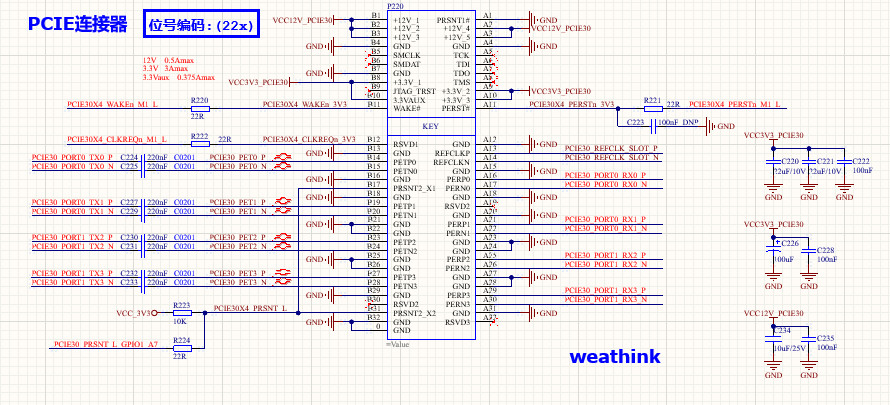
Figure 1: PCIe 4-Lane Slot
2. Clock Distribution
PCIe 3.0 requires an extremely stable 100MHz reference clock (REFCLK).
● Clock Buffer: The reference diagram uses a PI6C557-05BLE clock driver. It multiplies the 25MHz crystal signal and distributes multiple sets of differential 100MHz HCSL level signals.
● Bidirectional Distribution: * One set of signals (REFCLK0) is sent to the PCIe clock input of the RK3588J SoC. * Another set of signals (REFCLK_SLOT) is sent to pins A13/A14 of the PCIe slot.
● Matching Resistors: At the clock output, 33Ω series matching resistors (R244, R246, etc.) and 49.9Ω ground resistors near the receiver are usually visible to reduce signal reflection and ensure correct HCSL levels.
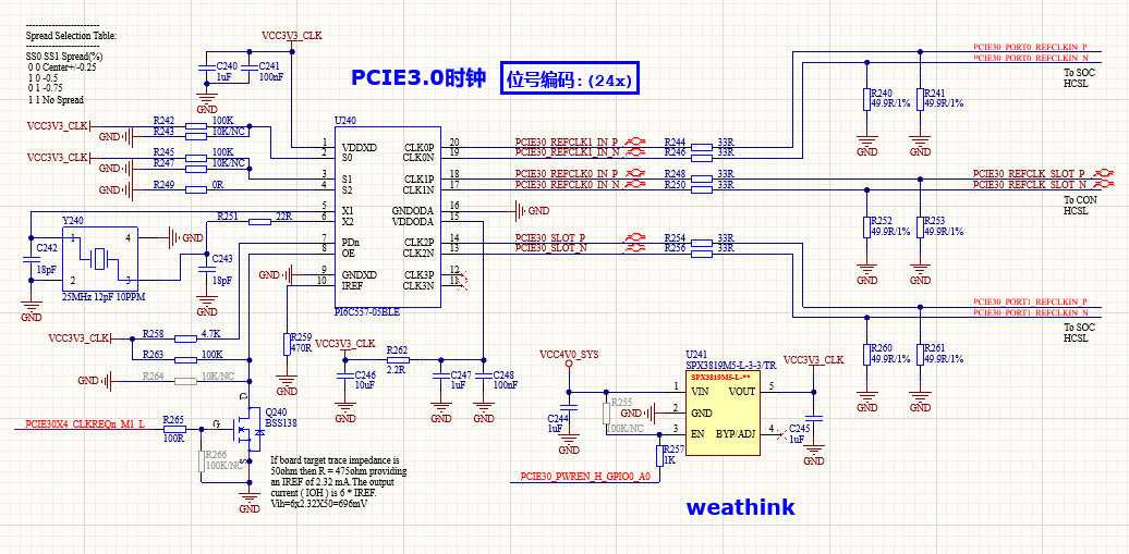
Figure 2: Clock Circuit
3. Power Management
The PCIe slot requires 12V and 3.3V power supplies, which usually need to be controlled by the SoC to achieve an orderly power-up sequence.
● DC-DC Conversion: Buck chips like the MP1653 are used in the diagram to convert the main power supply into the VCC3V3_PCIE30 required by PCIe.
● Power Enable: MOS transistors (Q200, Q201) are controlled via the SoC's GPIO (e.g., GPIO0_A0) to turn the slot power on or off. This is crucial for low-power management and circuit protection.
● Decoupling and Filtering: A combination of large-capacity electrolytic capacitors (100uF/220uF) and ceramic capacitors is configured at the slot power pins to handle surge currents during hot-plugging.
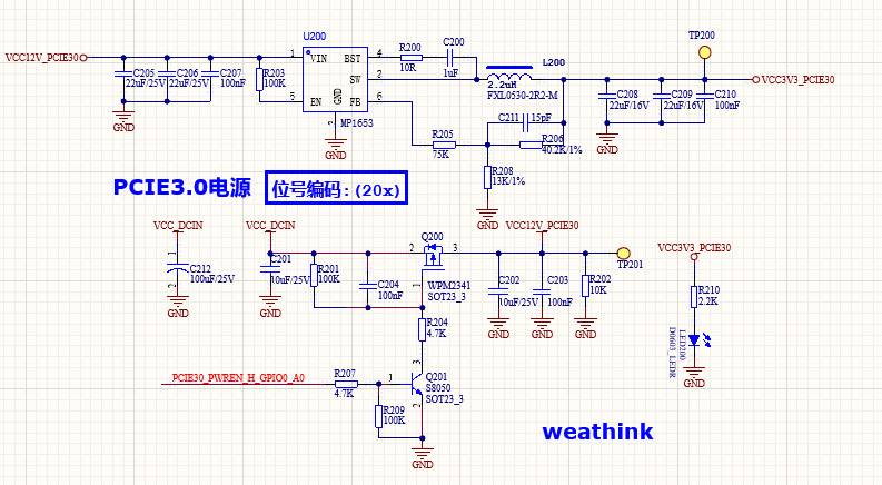
Figure 3: Power Circuit
4. Control Signals
In addition to high-speed data lines, the following signals are critical for establishing the PCIe link:
● PERST# (Reset): Reset signal. Issued by the SoC and sent to the slot after level shifting (e.g., 1.8V to 3.3V). The reference diagram uses C223 for simple RC delay filtering to ensure the system is stable when the reset is released.
● WAKE#: Wake-up signal. Supports devices waking up the host from a low-power state.
● PRSNT2# (Presence): Presence detection signal. This signal (such as pin B31 of the slot) is typically pulled up to 3.3V via a resistor and connected to a GPIO of the SoC. When a card is inserted, this pin is grounded, allowing the SoC to recognize that a device is connected.
● CLKREQ#: Clock request signal. Used to implement clock gating in the L1 substate to save power.
5. Design Considerations
● Length Matching: Intra-pair differential length matching should be controlled within 5mil. In x4 mode, inter-pair length matching should also be maintained as much as possible to reduce skew.
● Complete Ground Plane: Crossing splits under high-speed signal lines is strictly prohibited; they must have a complete reference ground plane.
● ESD Protection: In industrial-grade designs, it is recommended to add low-capacitance ESD protection devices to the PCIe slot signal lines near the connector.
Through the above design, the RK3588J can stably drive various PCIe 3.0 devices, such as NVMe solid-state drives, 10-Gigabit network cards, or FPGA acquisition cards.
6. Advantages of Using the Weathink WTC-RK3588-B SOM
In actual development, designing a full board directly based on the RK3588J chip is highly challenging. Adopting the Weathink WTC-RK3588-B System-on-Module (SOM) can significantly accelerate the process:
● Simplified Design: The SOM integrates the CPU, DDR, and power management. Developers only need to refer to Figure 1 (Connect.jpg) to design the baseboard, greatly reducing PCB layers and costs.
● Guaranteed Performance: The SOM has completed the most complex impedance matching and signal simulations, ensuring stable PCIe 3.0 operation at 8Gbps.
● Shortened Cycle: Combining a mature clock solution and power architecture allows developers to skip core system debugging, bringing products to market faster.