
Latest News


Schematic Design of Allwinner T153 Connecting to WIFI and BT (AP6212)
In embedded development, the AP6212 is a classic two-in-one WIFI/BT module (based on Broadcom chips) that supports 2.4G WIFI and Bluetooth 4.2. This article will provide an in-depth analysis of the core points of its schematic design based on the Allwinner T153 platform.
1. WIFI Interface Circuit: SDIO 3.0 and Power Supply Design
The WIFI portion of the AP6212 communicates with the main controller via the SDIO interface. The key to its stability lies in timing matching and power purity.
1.1 SDIO Signal Connection
According to the schematic design, the SDC3 interface of the T153 serves as the WIFI data link:
●Core Signals: These include SDC3-CLK, SDC3-CMD, and data lines SDC3-D0 through D3.
Series Matching: In the SDC3 link, matching resistors of 22Ω ~ 33Ω (such as R1000, R220, etc.) are connected in series at both the controller and module ends.
●Impedance Requirements: PCB routing must strictly control a 50Ω single-ended impedance. Furthermore, signals within the SDIO group must be processed with equal lengths, controlling the error within 200mil to prevent phase shifts during high-speed data transmission.
1.2 Power System Design
●Main Power Supply (VBAT): The AP6212 requires a stable power supply. In the schematic, the system VCC_3V3 is isolated into VCC_WL through the magnetic bead FB200.
●Filtering Protection: A large 22uF capacitor (C211) and a 100nF decoupling capacitor are configured at the module input to smooth out voltage drops during WIFI data burst transmissions (such as carrier startup).
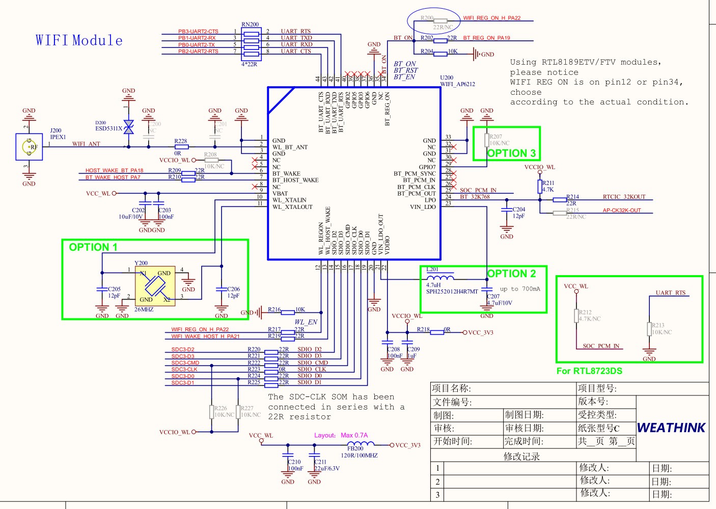
Figure 1 WIFI Partial Circuit
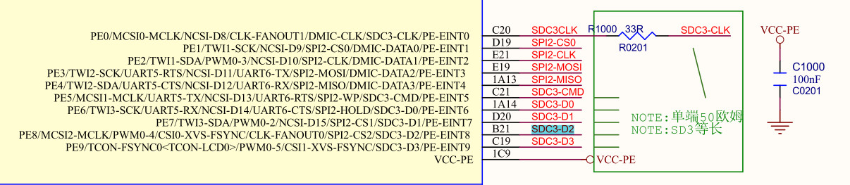
Figure 2 SDIO Circuit of SOM Part
2. Bluetooth Interface Circuit: UART, Clock, and Audio
The Bluetooth portion operates independently of the WIFI and performs control and data exchange through the UART interface.
2.1 UART and Hardware Flow Control
The AP6212 Bluetooth connects via the PB0-UART2 interface.
Four-wire Connection: Due to the large data throughput of Bluetooth, the design utilizes UART2-TX/RX as well as UART2-RTS/CTS. Hardware flow control effectively prevents FIFO overflow at high baud rates, ensuring that Bluetooth audio or file transfers do not drop.
2.2 Clock Circuit (LPO)
The Bluetooth module relies heavily on an external 32.768KHz clock during sleep and low-power modes:
Design Solution: OPTION 3 in the schematic provides an external Real-Time Clock (RTC) input path. If the main controller's RTC drive capability is insufficient, a 10KΩ pull-up resistor (R207) must be added to enhance the signal amplitude.
3. Control Signals and RF Terminal Processing
3.1 Enable and Wake-up Logic
●WIFI_REG_ON (PA22): High level enables the WIFI module.
●BT_REG_ON (PA19): High level enables the Bluetooth module.
●Interrupt Feedback: WIFI_WAKE_HOST (PA21) and BT_WAKE_HOST (PA7) are used to initiate interrupt signals from the module to wake up the Allwinner T153 controller when the system is in sleep mode, achieving low-power management for the entire machine.
3.2 RF Antenna Layout
An ESD5311X electrostatic protection tube is placed at the front end of the antenna socket (J200). During Layout, the RF traces should be as short and straight as possible. The reference ground plane must be complete and stay away from any switching power supply (DC-DC) areas.
4. Weathink: Professional Allwinner Solution Provider
As a deep partner of the Allwinner platform, Weathink possesses over a decade of experience in high-speed signal routing and industrial hardware design. We provide various core boards and customized industry solutions centered on the Allwinner T153. Combining extreme cost-effectiveness with professional technical support, we help customers achieve rapid productization in the fields of industrial control and edge computing.