
Latest News
-

T113 External SPI NAND Storage Solution
2026-07-03 -

Ethernet Schematic Design for Allwinner T113
2026-07-03 -

-

-

T113 External SPI NAND Storage Solution
In embedded system design, the selection of a storage solution is critical for product stability, boot speed, and cost control. As a highly integrated industrial-grade processor, the Allwinner T113-i is widely used in intelligent terminals, industrial control, and other fields. This article combines schematics to provide a detailed analysis of the circuit design implementation for T113 external SPI NAND storage.
1. System Solution Overview
The T113-i is equipped with flexible peripheral interfaces capable of supporting various storage media. With its small size, simple interface, and lower cost, SPI NAND Flash has become the preferred choice for many small and medium-sized embedded systems. This solution adopts the common SPI interface protocol, realizing communication with the SPI NAND chip through the PC port group of the T113.
2. Hardware Circuit Design Details
Based on the schematic, we can divide the hardware connection into two parts: the SOC-side configuration and the NAND Flash peripheral-side implementation.
2.1 T113 SOC-side Pin Mapping
The figure below shows the T113 PC port group multiplexed as SPI function pins. The specific pin correspondences are as follows:
●PC2 (SPI0-CLK): Provides the SPI clock signal.
●PC3 (SPI0-CS0): Chip select signal, used to activate the Flash chip.
●PC4 (SPI0-MOSI): Master Out, Slave In, used for data transmission.
●PC5 (SPI0-MISO): Master In, Slave Out, used for data reception.
●PC6 (SPI0-WP): Write protect pin. PC7 (SPI0-HOLD): Hold pin.
During PCB layout, these pins must strictly follow high-speed signal design guidelines to ensure signal integrity.
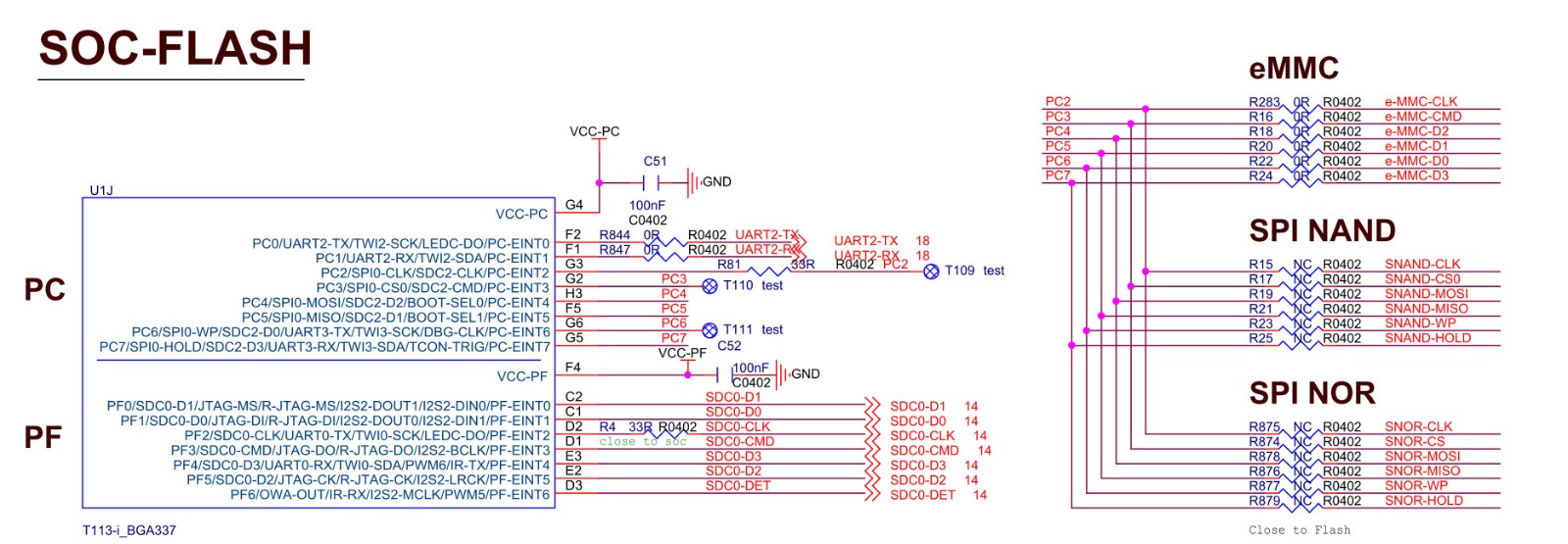
Figure 1: T113 SPI NAND Pins.
2.2 SPI NAND Peripheral Circuit Implementation
The figure below shows U39 (model XT26G01CWSIG, 128MB capacity) as the SPI NAND Flash chip used in the actual application.
●Power Supply Handling: Pin 8 (VCC) is connected to the system power supply VCC-PC through RM11 (0-ohm resistor), with a CM8 (100nF) capacitor for filtering to ensure stable power supply.
●Signal Matching and Pull-up: To ensure a determined signal state when the bus is idle, the schematic uses 10K-ohm resistors (RM14, RM13, RM12) to pull the SNAND-WP, SNAND-CS0, and SNAND-HOLD pins up to VCC-PC, enhancing anti-interference capability.
●Grounding Design: Pin 4 (VSS) and EPAD are connected directly to the system ground (GND), ensuring a good signal reference plane.
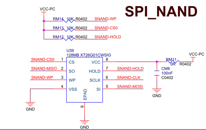
Figure 2: External SPI NAND.jpg
3. Design Considerations and Suggestions
In actual routing and debugging, it is recommended to pay attention to the following points:
●Trace Length: When the SPI clock frequency is high, the trace length the SOC to the Flash should be shortened as much as possible to avoid signal reflection and crosstalk.
●Pull-up Resistor Placement: Pull-up resistors should be placed as close to the Flash chip pins as possible.
●Power Stability: SPI NAND is sensitive to power ripple; pay attention to the integrity of the power plane.
4. Conclusion
In the development practice of the T113 a reasonable storage circuit design is the foundation for ensuring system stability. As an Allwinner solution design company, Weathink has accumulated extensive practical experience in the design and debugging of various NAND storage solutions. Underlying signal integrity optimization to driver compatibility debugging, we can provide customers with efficient technical support to help your products achieve superior storage in industrial scenarios.