
Latest News


RK3568 Device Tree Configuration for LVDS LCD Display Driver Technical Guide
Abstract
This article provides a detailed guide on configuring the LVDS (Low-Voltage Differential Signaling) LCD display driver on the Rockchip RK3568 processor in a Linux environment through the device tree. We will delve into the principles of the LVDS interface, key nodes in the device tree, timing parameter configuration, and troubleshooting common issues. This guide aims to provide hardware and software engineers with a comprehensive and practical configuration method to ensure the stable and efficient operation of the LVDS LCD display on the RK3568 platform.
1. Overview of RK3568 and LVDS LCD Displays
The Rockchip RK3568 is a high-performance, low-power general-purpose SoC, widely used in smart NVRs, cloud terminals, IoT gateways, industrial control tablets, and other applications. It integrates powerful multimedia processing capabilities and supports various display interfaces, with LVDS being a commonly used interface in industrial and automotive fields due to its strong anti-interference capability, long transmission distance, and low power consumption. The LVDS LCD screen transmits image data through differential signals, requiring precise timing and proper configuration to display correctly. In a Linux system, the device tree is the core mechanism for describing hardware information. For complex SoCs like the RK3568, all peripheral configurations, including display controllers and LVDS interfaces, are handled via the device tree. This guide will use a BOE LCD screen (model: EV101WXM) as an example, based on the WTC-RK3568 core board hardware.
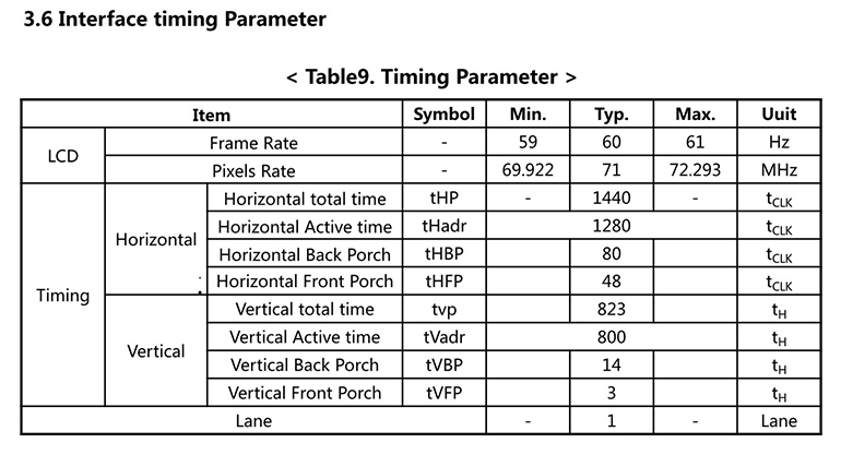
Figure 1: LCD Timing Parameters
2. Basic Device Tree Configuration
The device tree is a data structure used by the Linux kernel to describe hardware topology. For the RK3568, the device tree files are usually located in the kernel source directory: arch/arm64/boot/dts/rockchip/, for example, rk3568-evb.dts or rk3568-xxx-board.dts. Configuring the LVDS LCD display driver mainly involves the following aspects:
●LVDS Controller Configuration: The LVDS controller within the RK3568 is responsible for generating LVDS signals.
●LVDS PHY Configuration: The LVDS physical layer (PHY) is responsible for converting digital signals to LVDS differential signals.
●Panel Information: Describes the specific parameters of the connected LVDS LCD, including resolution, timing, backlight control, etc.
●Display Routing Configuration: Ensures that display data is routed correctly from the RK3568 internal display controller to the LVDS output.
3. Key Device Tree Nodes and Attributes for LVDS Configuration
In the RK3568 device tree, configuring the LVDS LCD typically involves the &lvds node and the lvds-panel subnode.
3.1 LVDS Controller Node (&lvds)
This node primarily configures the operating mode of the LVDS controller and its connection to the panel.
&lvds {
status = "okay";
ports {
#address-cells =<1>;
#size-cells =<0>;
port@1 {
reg =<1>;
lvds_out_panel: endpoint {
remote-endpoint = <&panel_in_lvds>;
};
};
};
};
Explanation of Key Attributes:
●status = "okay": Enables the LVDS controller.
●ports: Defines the connection between the controller and the panel. lvds_out_panel is the LVDS controller's output endpoint, which connects to the panel’s input endpoint panel_in_lvds.
3.2 LVDS PHY Node (&lvds_phy)
The LVDS PHY is typically a separate module within the RK3568 responsible for the physical layer characteristics of the LVDS signal.
&lvds_phy {
status = "okay";
rockchip,grf = <&grf>;
rockchip,phy-supply = <&vcc_3v3>;
};
Explanation of Key Attributes:
status = "okay": Enables the LVDS PHY.
rockchip,phy-supply: Specifies the power supply for the LVDS PHY, which must be configured according to your hardware schematic.
3.3 Panel Node (lvds-panel)
This node configures core parameters for the LVDS LCD, including resolution, timing, backlight, and power sequencing.
lvds-panel {
compatible = "simple-panel";
power-supply = <&vcc_3v3>;
backlight = <&backlight>;
enable-gpios = <&gpio0 rk_pc5="" gpio_active_high="">;
prepare-delay-ms =<20>;
enable-delay-ms =<20>;
disable-delay-ms =<20>;
unprepare-delay-ms =<20>;
bus-format =
width-mm =<217>;
height-mm =<136>;
display-timings {
native-mode = <&timing0>;
timing0: timing0 {
clock-frequency =<71000000>;
hactive =<1280>;
hback-porch =<80>;
hfront-porch =<48>;
hsync-len =<32>;
hsync-active =<0>;
vactive =<800>;
vback-porch =<14>;
vfront-porch =<3>;
vsync-len =<6>;
vsync-active =<0>;
de-active =<0>;
pixelclk-active =<0>;
};
};
port {
panel_in_lvds: endpoint {
remote-endpoint = <&lvds_out_panel>;
};
};
};
Explanation of New Attributes:
●prepare-delay-ms, enable-delay-ms, disable-delay-ms, unprepare-delay-ms: These parameters define delays for the panel’s power and enable sequencing, ensuring the panel powers on, enables, disables, and powers off at the correct times.
●bus-format =
width-mm, height-mm: Physical dimensions of the panel used for DPI (dots per inch) calculations.
de-active: Polarity of the data enable signal.
3.4 Display Routing Node (&lvds_in_vp1, &route_lvds)
These nodes manage the routing of display data within the RK3568, ensuring the image data is sent from the video processor to the LVDS controller.
&lvds_in_vp1 {
status = "okay";
};
&route_lvds {
status = "okay";
charge_logo,mode = "center";
connect = <&vp1_out_lvds>;
};
Explanation of Key Attributes:
●&lvds_in_vp1: Represents the path for the LVDS signal into video processor 1.
●&route_lvds: Defines the routing of LVDS display data, including the charging logo mode and which video output port to use.
3.5 Other Display Controller Status (&dsi0, &dsi1, &video_phy0, &video_phy1)
Depending on your configuration, other MIPI DSI controllers may be disabled while specific video PHYs are enabled.
&dsi0 {
status = "disabled";
};
&dsi1 {
status = "disabled";
};
&video_phy0 {
status = "okay";
};
&video_phy1 {
status = "disabled";
};
Explanation of Key Attributes:
●&dsi0, &dsi1: Explicitly disables MIPI DSI controllers, indicating that LVDS output is managed through a separate LVDS controller (&lvds).
●&video_phy0, &video_phy1: Controls the status of video PHY interfaces. Enabling video_phy0 is typically associated with the LVDS output path.
4. Backlight Configuration
The LVDS LCD typically requires separate backlight control. The RK3568 can control backlight brightness via PWM or GPIO.
4.1 PWM Backlight Control
&pwm5 {
status = "okay";
};
backlight: backlight {
compatible = "pwm-backlight";
pwms = <&pwm5 0="" 25000="">;
brightness-levels = <...>;
default-brightness-level =<200>;
post-pwm-on-delay-ms =<10>;
pwm-off-delay-ms =<10>;
status = "okay";
};
4.2 GPIO Backlight Control
backlight: backlight {
compatible = "gpio-backlight";
gpios = <&gpio0 rk_pb1="" gpio_active_high="">;
default-on;
status = "okay";
};
Complete Device Tree Example (Based on Your Configuration)
The following is a complete example of the RK3568 device tree configuration based on the provided configuration snippet.
Compiling and Flashing the Device Tree
After modifying the device tree, you need to recompile the device tree and flash it to the RK3568 device.
5. Conclusion
This detailed guide should help you gain a deeper understanding of configuring the LVDS LCD display driver for the RK3568. The key is to match the timing parameters from the LCD datasheet and configure the RK3568's internal LVDS controller, PHY, and display routing correctly. In practical development, using the Weathink RK3568 core board can simplify hardware complexity, allowing you to focus more on software configuration and debugging. Patience and a deep understanding of the hardware are key to success. I hope this guide helps you successfully light up the LVDS LCD and accelerate your RK3568 project development.
If you have any questions about the RK3568 hardware design, LVDS LCD driver, or Weathink RK3568 SOM during your project development, or need deeper technical support or custom services, feel free to contact us:
Contact: Mark
Email: lw@weathink.com
Phone: 18072728558