
Latest News
-

-

-

-

-

Rockchip RK3568 External SD Card Design
2025-02-13
HDMI Interface Schematic Design for Rockchip RK3568
The Rockchip RK3568 is a high-performance, versatile processor widely used in industrial control, consumer electronics, and embedded devices. HDMI, as a mainstream interface for modern display systems, supports high-resolution video and multimedia functions. This article provides a detailed explanation of the HDMI interface schematic design for RK3568, including its principles, design details, and key considerations.
1. Principles of the HDMI Interface
HDMI (High Definition Multimedia Interface) is a fully digital interface used for transmitting uncompressed audio and video signals. It is commonly used in devices such as set-top boxes, DVD players, personal computers, gaming consoles, digital audio systems, and televisions. HDMI supports simultaneous transmission of audio and video over a single cable, simplifying system wiring.
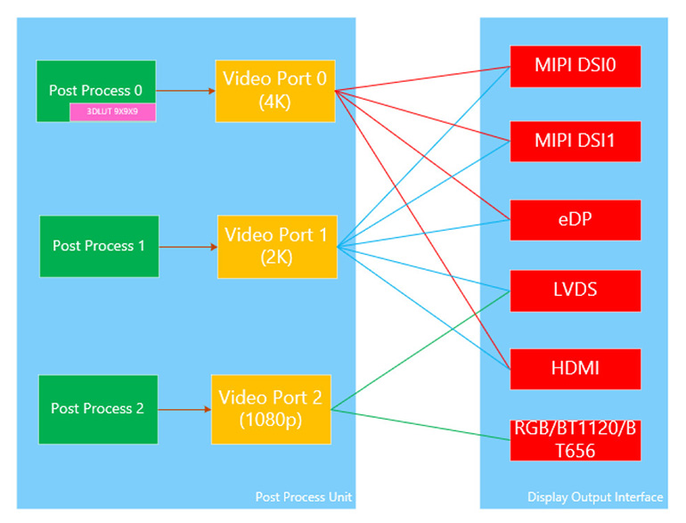
Figure 1: The connection relationship between RK3568 VOP and display interface
The RK3568 features three independent Video Ports (VOP), with the HDMI interface connected to either VP0 or VP1. Internally, the HDMI interface generates TMDS differential signals through its video processing unit, which are then output to external HDMI display devices.
2. HDMI Interface Schematic Design
2.1 HDMI Signal Output Pins
RK3568 provides dedicated HDMI signal pins for outputting TMDS differential and control signals. Key pins include:
●TX0±, TX1±, TX2±: Three pairs of TMDS data differential signals.
●TXC±: TMDS clock differential signal pair.
●HPD (Hot Plug Detect): Used to detect whether an HDMI device is connected.
●DDC (Data Display Channel): Communicates with display devices via I2C to transmit EDID information and HDCP keys.
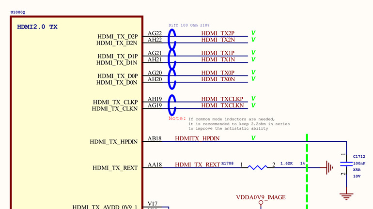
Figure 2 About the HDMI pins of RK3568
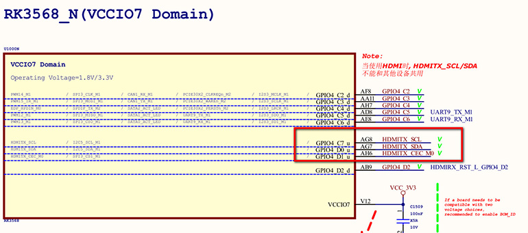
Figure 3 About the HDMI I2C pins of RK3568
2.2 TMDS Differential Signal Pair Design
●Impedance Control:TMDS differential pairs must have an impedance of 100Ω ±10% to ensure signal integrity.
●Equal-Length Routing:Differential signal pairs must maintain equal lengths, with a maximum deviation of less than 0.15mm, to avoid signal delay and distortion.
●Shielding:Signal traces should be routed close to the ground plane to minimize electromagnetic interference.
2.3 I2C Signal Design
The RK3568’s DDC interface uses an I2C bus for communication with the display device. Design considerations include:
●Adding 4.7kΩ pull-up resistors to the SDA and SCL lines.
●Minimizing the length of signal traces to reduce attenuation.
2.4 Power Supply and ESD Protection
Power Supply
HDMI requires a 5V power supply (HDMI_VCC) to power external display devices. Decoupling capacitors (0.1µF and 10µF) should be added to filter high-frequency noise.
ESD Protection
Add ESD protection components (e.g., TVS diodes) to power and signal lines to protect the chip from static electricity damage.
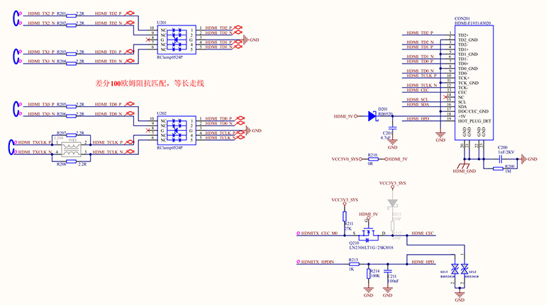
Figure 4 HDMI connector interface
3. Summary
The HDMI interface design for Rockchip RK3568 enables high-quality video and audio output through proper circuit design. This article detailed the HDMI pin assignments, circuit design highlights, and PCB routing considerations, providing valuable guidance for developers. By following these design and validation steps, developers can create a stable and reliable HDMI interface, enhancing multimedia functionality in embedded systems.
Weathink Electronics Co., Ltd., as a professional motherboard design company, adheres strictly to chip requirements in circuit design. For any issues, feel free to contact us. The WTB-RK3568S industrial control board provided by Weathink is based on our independently designed RK3568 SOM ensuring stability and reliability.
WTB-RK3568S SBC: https://www.weathink.com/products/danban/14.html